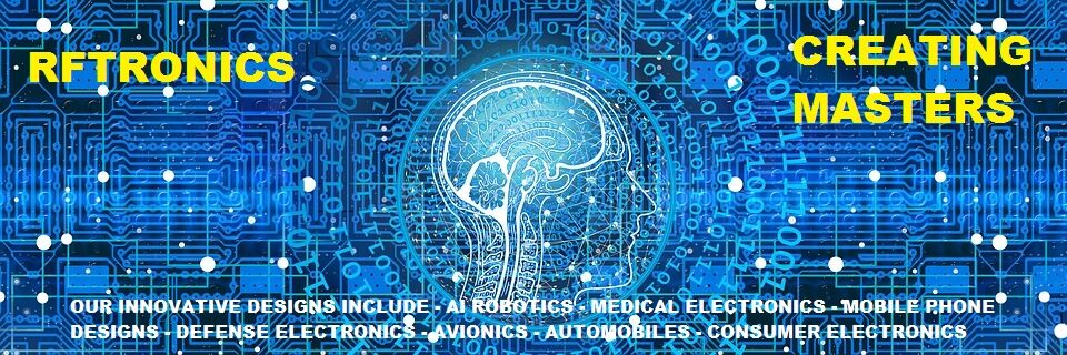
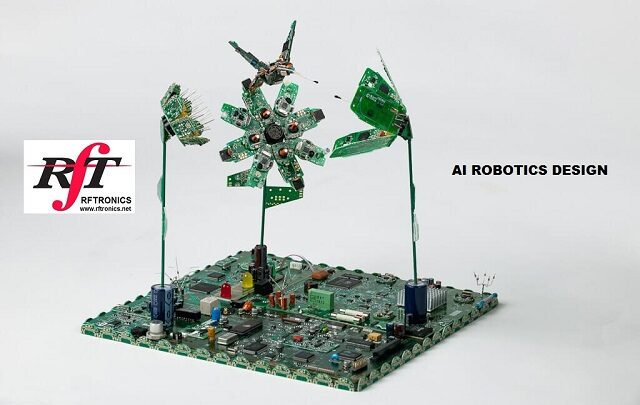
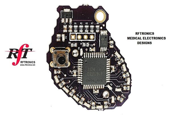
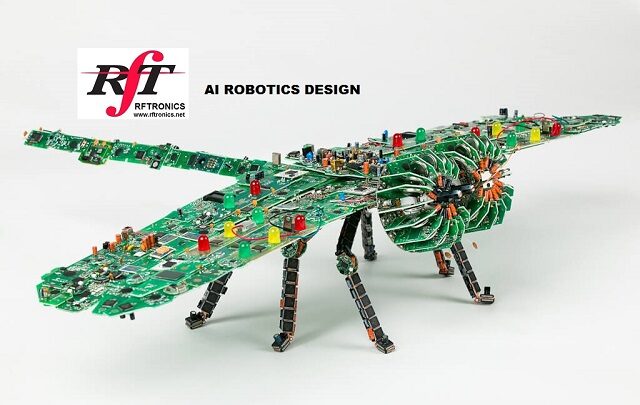
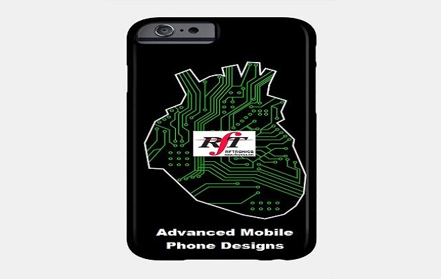
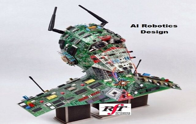
OUR INNOVATIVE DESIGNS INCLUDE - AI ROBOTICS - MEDICAL ELECTRONICS - MOBILE PHONE DESIGNS - DEFENSE ELECTRONICS - AVIONICS - AUTOMOBILES - CONSUMER ELECTRONICS


PCB Design solutions in RFTRONICS.,
A Few Steps ahead to Innovate your thoughts, Renovate your ideas, Rejuvenate your establishments
We have been providing design services for the development of futuristic technology for both Public and Private sectors in India within a short span of time. PCB services from the initial stage of Conception to last stage of Manufacturing and Production are provided with a desire to bring the best within us to offer complete Engineering Solutions. With a zeal to excel in designing most complex and challenging boards within the given time frame and having customer satisfaction as our primary aim, our Engineering Team works 24x7 providing services in-house as well as on-site as per the design requirements of the clients.
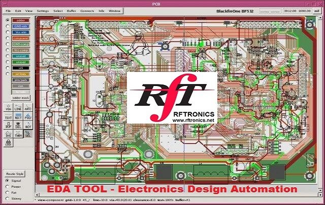
PCB DESIGN SERVICES
RFTRONICS's core competency is its PCB design capabilities. More than 50 highly skilled PCB layout engineers working with world-wide customers deliver "First time right designs”. The stringent process, continual training programs on current technologies are the keys for the success of the company. The experience acquired from handling highly complex PCB designs for cutting-edge technologies spread across major Industry Verticals like Military, Aerospace, Telecom, Medical, Automotive, Industrial and consumer electronics. “Quickest Turnaround Time”- With flexible working hours, multiple resources, shifts (24 X 7), skill programs and Stringent Quality Checks, ensure that extreme turnaround time challenges are achieved for customers. Our established design credentials combined with world class prototyping facilities makes the logical design into a working printed circuit board in the quickest Turnaround Time! This made RFTRONICS the leading PCB Design Engineering Centre for most of the leading Multinational R&D's.
DIFFERENTIATING FACTORS
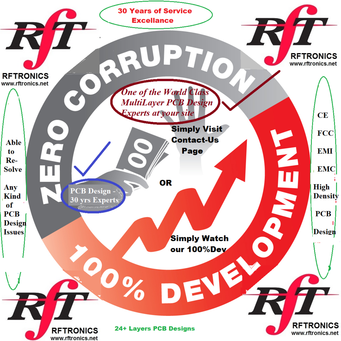
- Over 1000 complex and HDI designs completed in 30 years.
- Expertise in High speed digital, Mixed signal, Analog & Power boards.
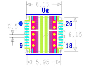
- Innovative design methods in Fine Pitch Micro BGA designs.
- Handled upto 0.37mm BGA pitch designs with 2 mil/ 2mil track/spacings.
- Design technologies with stacked and staggered µ via HDI technology.
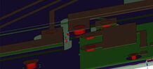
- Integrating Mechanical & Electrical CAD data for assembly verification.
- Board level, System level SI , PI, EMI/EMC & Thermal analysis.
- High bit rate (~ 28Gbps) analysis for serial I/O designs.
- Signal performance analysis for Reflections, Timing, BER, EYE opening.
- DC drop analysis in power supply rails due to copper losses.
- ISO 9001: 2015 CERTIFIED.
- Custom Programs: Over the years we have developed custom programs and scripts to gain efficiencies, improve quality and augment the current design tools.
PRODUCT DESIGN & DEVELOPMENT
The new product development process for our electronic products are in compliance to all required Global Certifications like CE,FCC Class A & Class B. These Certification requirements are achieved by our Innovative Product Development Team using EMI / EMC guidelines plus Signal Integrity Techniques.
LIBRARY SUPPORT
Our dedicated library team produce highly accurate symbols & parts needed for PCB design with stringent quality checks and quick turnaround. More than 15,000 validated component libraries help customers to start PCB designs instantaneously. Library Support is available online for customers with status and availability information of components in the master database.
Benefits
- IPC-7351 compliant , IPC naming conventions
- Standardized properties across all tool sets
- Adoption to any required tool sets
|
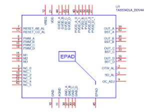
Symbols Salient features |
Footprints Salient features |
||||||||||||||
|
- Mandatory/defined attributes in every Symbol. |
|
||||||||||||||
|
|
||||||||||||||
| Example Symbol | Example Complex Footprint | ||||||||||||||
|
|
|
||||||||||||||
 |
 |
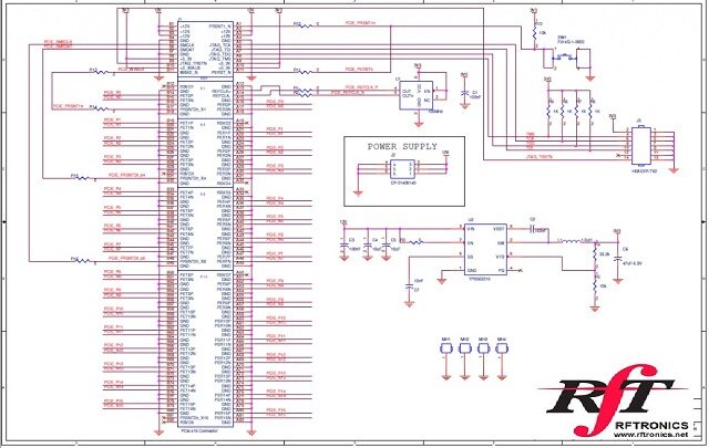
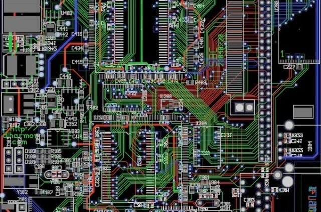
SCHEMATIC DESIGN DEVELOPMENT
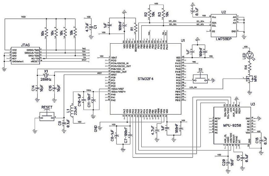
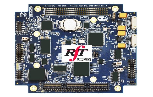
PCB DESIGN AND PROTOTYPE MODULE
QUICK TURN PROTOTYPE
Complexeties Handled
- PCB Thickness : upto 4.2 mm
- PCB Layers Handled : 24 Layers
- POP: 0.4mm & 0.6mm pitch
- BGA's:
-- Pitch: 0.4mm
-- Ball Size: 0.2mm
-- No of Balls: 2800 - QFP's:
-- Pitch: 0.38mm - Discrete Packages: Up to 01005 (0.41mm x 0.20mm)
- Place component package 0201 at 45° angle
- 40 BGAs in an assembly
- Max. Component Count/ Board: 10k
Active Member of Anti-corruption Team
PAGE VIEWERS
7 1 1 7 0 5
PRODUCTS
BOARD DESIGN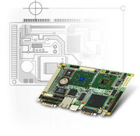
TESTING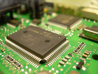
PRODUCTION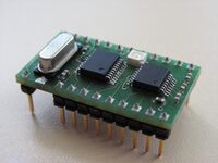
TOOLS
TOOLS
 |
|
Cadence Allegro: Users of cadence tool suites since 2000. Support all 14.X version to latest versions. Expertise in handling very complex designs. Capability to reduce design cycle time by 50%. |
 |
|
Mentor Graphics Expedition, Power PCB (PADS), Boardstation and all schematic tool configurations |
 |
| Altium: Support all latest releases. |
 |
SIGNAL INTEGRITY
SIGNAL INTEGRITY
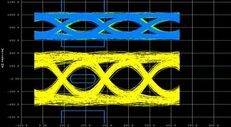
*Experience of handling prelayout & postlayout designs/topologies helps
customer to first time right designs.
*Successfully executed complex Multidrop/Multipoint topologies.
*Asserting PCB layer stackup/Layer ordering/PCB materials based on SI results.
*Validating the logic level, Drive strengths, Termination techniques,
Thresholds, Over/Under shoot, Propagation Delay, Noise margin etc., Slew
Rate, Timing Budget(setup/Hold time), EYE Diagram.
*BER, ISI, Jitter, Loss(IL,RL) analysis.
*Cross talk analysis and mitigation methodologies.
*SerDes/DDRx/XAUI/PCIe interfaces.
*Handled upto 12.5Gb speed.
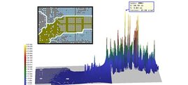
EMI/EMC ANALYSIS
EMI/EMC ANALYSIS
*Expeienced in Board level & System level EMI Analysis.
*Frequency V/S dB plot for Different standards
(FCC, CISPR, VCCI or User specific)
*RE/CE analysis to find out how much the product is emitting.
*RI/CI analysis to find out how much the product can withstand external
radiation.
*3D Magnetic/Electric & Current density Plots
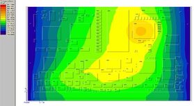
POWER INTEGRITY
POWER INTEGRITY
*IR/DC Drop analysis with Voltage/Current Density 3D plots
*Decoupling Analysis with Frequency V/S Impedance plot
*Plane Noise Analysis with 3D plot of plane noise
THERMAL ANALYSIS
THERMAL ANALYSIS
*Detailed reports indicating component and board temperature profiles
*Heat sink and cooling proposals
*Metal core and thermal ladder PCB designs
*Mean time between failure study
*Major heat transfer mechanisms analysis viz., Conduction, Convection,
Radiation